FET Audio | Hi-End Audio & Electronics DIY Electronics & Repair

October 29, 2009

D1V3 & D1V33 upgrade to 24bit input mode

Filed under: DAC — Spencer @ 3:02 pm

I remember there is one diyer of D1V3 told me that D1 is not able to receive true 24 bit digital data format.  The reason is that D1 has choosen to use 18 bit modes for CS8414 and SM5842.  In order for D1V3 and D1V33 to receive 24 bit data, I have tried out successfully to use the 24 bit Right Justified mode for both DIR9001 and SM5842.  Below is the details.

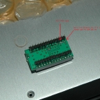
For DIR9001, set Pin 25 FMT0=H and Pin 26 FMT1=L means 24 bit Right Justified output data mode.  This is a easy setting by J1 short and J2 open on the DIR9001 converter board.

For SM5842,  the pin 5 IW1N and Pin 10 IW2N  has to be both Low (GND) for 24 bit data input mode right justified.  In the design of the pcb, there is no jumper setting for SM5842 IW2N (pin 10) which is always tie to +5V (High).  Thus the follow procedure has to be done to make the change to 24bit data input mode.

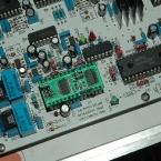
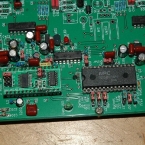
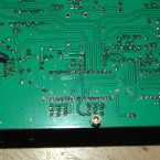
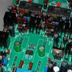
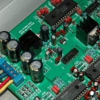
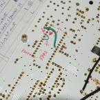
  1. Cut the trace on the bottom of the pcb on both sides of the pin 10 trace as shown.  Cut two line with 1mm width and remove copper in between as in the picture.  Check with ohmmeter for open circuit.
  2. Solder a wire from the Pin 10 of SM5842 to Pin 8 which is ground pin (thin blue wire).
  3. Connect a wire (thick green wire) from +5V supply of SM5842 to the jumper side as show in the pictures.  This is to ensure the jumpers has the +5V supply as usual.
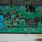
  4. On component side, set J22 to 8414 (18bit) side, i.e. Pin 5 become Low (Ground).

FFT measurements show that the different between 16 and 20 bit signal noise floor is more than 12 db at -80dbFS input for PCM63 DAC.  This proved that the digital data input 24bit right justified mode is working!

For PCM1704, the lowest noise floor is about -132dbV with 24 bit -90dbFS data input.

FFT DAC D1V33 16 vs 20 bit PCM63

FFT DAC D1V33 16 vs 20 bit -80dbFS PCM63

DAC D1V33 63 vs 1704 at FS 24bit

FFT DAC D1V33 1704 at -90dbFS 24bit

Update Mar 13, 2010:

For PMD100 converter board, cut trace between pin 12 and 13.  Short the pin 13 to pin 14 (ground) – PMD100 set to 16 to 24 bit input mode with Left Justified.

Set jumper of DIR9001 J1 – open and J2 – short; this is to set Left Justified output mode for DIR9001.

*** Do not do below change for PCM63 user ***

If you want to change the PMD100 converter board to 24 bit ouput mode (for PCM1704), you have to set pin 10 from L (ground) to H (5V).  The problem with the converter board is that the top and bottom of pin 10 is shorted to ground plan.  Thus you have to cut both trace on top and bottom but it is impossible to modify if you have soldered the chip or IC socket! 

Short pin 10 to pin 11 if you can isolated the ground connection on pin 10.  Then you have 24 bit output mode.
Related Images:

October 27, 2009

PCM1704 to PCM63 Converter BD

Filed under: DAC — Spencer @ 10:43 pm

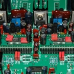
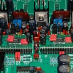
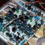
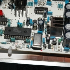
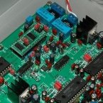
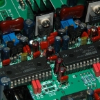
Since I have a PCM1702 to PCM63 converter board pcb, I have put a PCM1704 on same adaptor board for testing purposes.  The only difference is two supply pins +/-5V need to be reversed.  Thus I do cut trace and add two hard wires at the bottom of the board to fit the supply reverse for PCM1704 DAC chips.

For Capacitor, I use Panasonic FC and also Wima MKS film capacitor for supply decouple as in the pictures.

For PCM1704, the noise floor is a bit lower as you can see from the FFT measurement.

D1V33 FFT with PCM1704

D1V33 FFT with PCM63 lin

Related Images:

September 11, 2009

D1V3 + Squeezebox Classic (SB3)

Filed under: DAC — Spencer @ 1:00 am

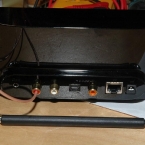
This is a modification of SB3 clock to sync to D1V3 on board super clock 11.2896MHz XO.

  1. Major improvement on D1V3 is to use a clean super clock for SM5842AP.
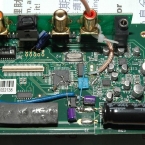
  2. Major problem is to connect the D1V3 super clock back to SB3.  Thus SB3 internal modifications are needed.  SMA coaxial cable is connected to pin 9 of HCU04 IC and ground.
  3. A separate 3.3V AMS1117 regulator is used for the CPLD and HCU04 ICs.  Sanyo OS-con and film cap are used for supply bypass.
  4. A linear 5V 1.5A regulator is used to replace the original switching adapter.

With this modification, the SB3 will not be able to play back other sampling frequencies file other than 44.1kHz!  Thus it is only good for CD playback now.

Some measurements:

SB3 SPDIF digital out FFT @ 1kHz

SB3 SPDIF digital out FFT @ 18kHz

D1V3 and SB3 FFT @ 1kHz (D1V3 analogy output)

D1V3 and SB3 FFT @ 18kHz (D1V3 analogy output)

Related Images:

June 11, 2009

D1V33 DAC

Filed under: DAC — Spencer @ 1:12 am

This is D1V33 completed in April 2009 and currently is still on sales.

Price refer to “D1V33 BOM” and Kit details refer to “D1V33 Assembly Manual” below:

Documentation:

D1V33 Silk Top

D1V33 Circuit Diagrams

D1V33_BOM *Updated on Jan 15, 2010*

D1V33 Assembly Manual

D1V33 FFT 1

D1V33 FFT 2

D1V33 FFT with PCM1704

Related Images:

September 11, 2008

Yamaha DA202 DA Converter

Filed under: DAC,Pro Audio — Spencer @ 10:34 am

Update on Nov 12, 2009:

FFT measurement:

DA202 FFT 16 vs 20bit 44.1kHz

DA202 FFT 16bit -10dbFS

DA202 FFT 16 vs 18bit -80dbFS

 So you can see the noise floor is not great at about -110dbV.

Last update on Sep 11, 2008:

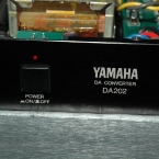
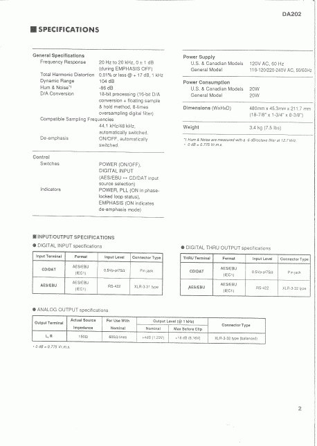
This is a professional DAC made by Yamaha back in 1988.  It was made for the DMP7D digital mixer in the same period using PCM56P-K x 2 and IC op-amps JRC 2068 and NE5532.  Yamaha use a custom IC YM3023 to switch the 16bit DAC into 18bit. The digital receiver chip is Yamaha YM3623B.  The power supply is a linear regulator.

DA202 Spec

Related Images:

« Newer PostsOlder Posts »

Powered by WordPress