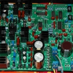
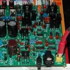
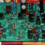
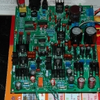
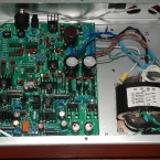
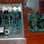
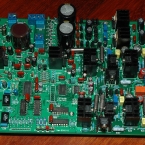
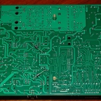
The DAC is base on the circuit of the hardwire version with some additional features.
- Digital Input: I2S (via pin header), SPDIF – RCA, AES and Toslink (optical); selected by two pins 00/01/10/11 for all 4 inputs. Default input is RCA – SPDIF without selector sub-pcb.
- Output: RCA Left and Right (about 1.5Vrms); mute by relay shorting output signal to ground
- Display: 3 LED – Mute, 48k, 96k; Fs display is for 8416 only!
- For Analogy Balance output, two pcb are required and one pcb jumpers will be set to Mono L and the other set to Mono R channel. I2S flat cable is reqired to connect the source pcb to the slave pcb. To be tested!
- Power input: 18V x 2 0.5A and 9V x 1 0.5A AC
This is the first version and thus there are few minor errors on the pcb: Optical input reversed pin 1 and 3 connection, no mounting holes for optical receiver, no mounting holes for XLR female socket, and non-optimized ground path. Thus some cut trace and jumper wires are reqired on the bottom of the pcb. But anyway the FFT measurement is quite satisfactory after error corrections. Here are the photos and FFT measurements.
From the FFT, you can see the noise floor is about -135dBV (-138dbr). It is about 5dB better than the hardwire version.
1794 DAC V1 FreqResponse & Distortion
Distortion and frequency is about same for both hardwire and Pcb version 1.
Update: June 30, 2010
One pcb is install in the casing and use a better transformer. The FFT is ploted again and 50Hz hum is not seen anymore.
D-A FFT DAC 1794 V1 log (Case set1)
