FET Audio | Hi-End Audio & Electronics DIY Electronics & Repair

November 23, 2012

F5T Turbo Power Amplifier kit for sales

Filed under: Pass Amplifiers — Spencer @ 11:01 pm

Those who had brought my F4 kits few years ago can purchase this kit or boards for a quick conversion from F4 into F5T because all the holes and mosfet locations will be same as the F4 pcb.  The optional MUR3020W can be obmitted if not use.   If F4 buyer has the original IRF9240/240 power mosfet, it can be re-used.

The To-92D transistor are Toshiba 2SC2705Y/2SA1145Y rated at 800mW and thus it is very safe to use at 60 deg C environment for less than 200mW dissipation.  It would survive safely under a maximum supply voltage of +/-32V.  The Panasonic capacitor is rated at 35V and thus a supply voltage of no more than +/-32V is recommended for this kit.

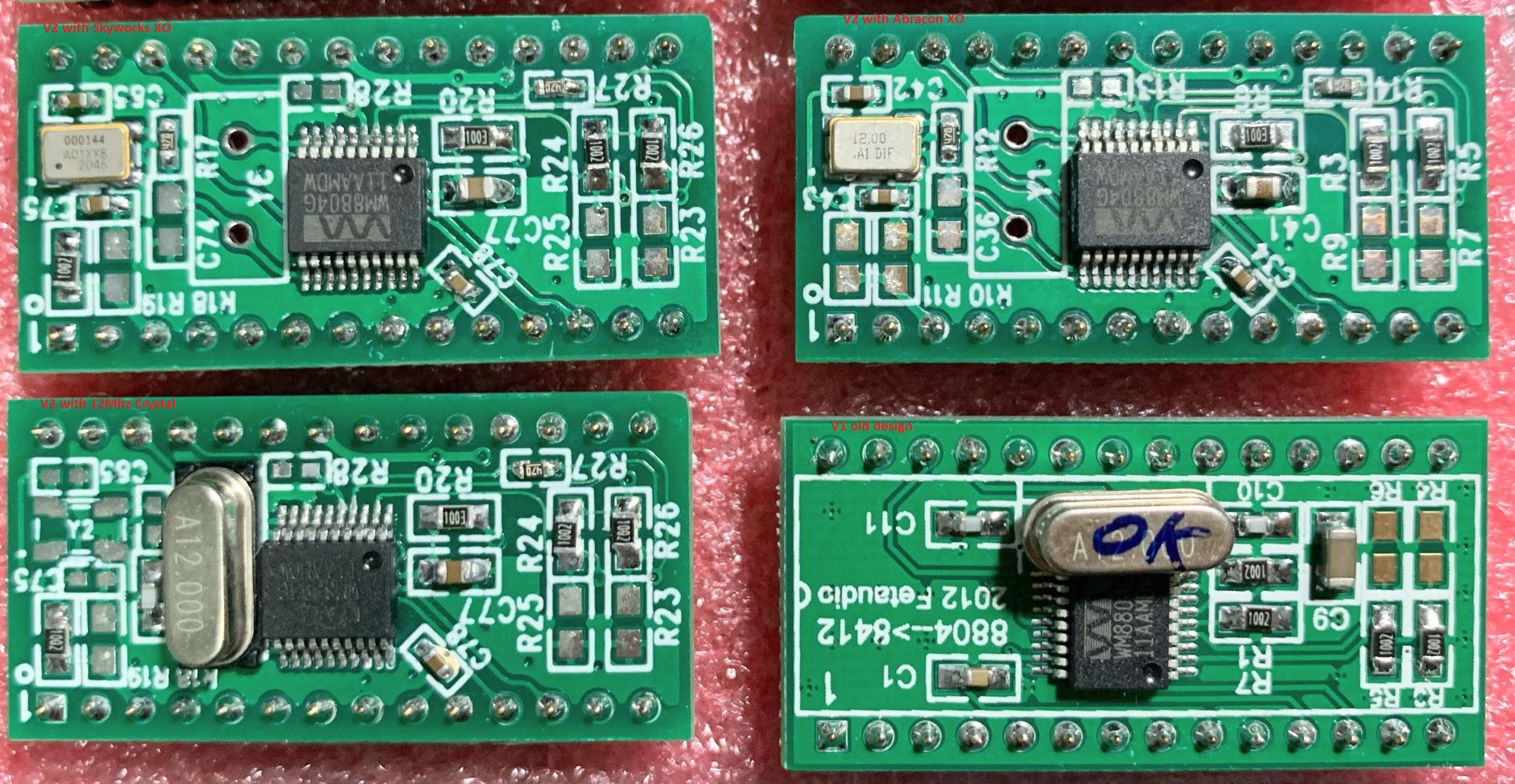
I build a version using Toshiba Mosfet 2SK1530/2SJ201.  The supply voltage is +/-22V and thus I do not use the cascade transistors (2SC2705Y and 2SA1145Y).  I also change 3 resistors and details refer to the “F5T-BOM-cost” document.  The change on R11/R12 is to increase the thermal stability and R27/R28 is for increasing the supply voltage to jfets to be minimum 10V or above for a supply voltage of 22V.  49.9R to replace 47R do to stock issue.

Sound wise, it is more powerful than the F5 original due to higher current output and more pairs of mosfet is used.  Overall the sound is smoother and warmer than F5. Nelson said this amp sound more relax!

Please look at the F5T-BOM-cost documents for the detail kits offer – Price & BOM options.

Details: F5T-BOM-Cost_2017 (updated transistors prices)

Manual: F5 Turbo Assembly Instruction v3

Power supply ripple comparison CLC vs CRC: It can be seen that an inductor of 0.47mH air-coil has improved the ripple peak to peak level to 20 times smaller.  See attached: F5T ripple

After building another set with Cascade transistors, the noise level with grounded input is about half of that without cascade transistors.  The reason is that the filtering of the transistors at the base is much better and thus the jfets is supplied with a more stable supply with lower noise level.  Here is the measurement comparison.

Notes for F4 up-graders:  For the MUR3020W, I have no pre-tap holes for them and thus I use a L-Bar to fix the 3 power mosfet and MUR3020W as shown.

I have built the third set with 32V supply as suggested by Nelson Pass.  Here is the measurement of distortion vs Power Output at 8.2 ohm load.  With higher supply voltage, the distortion is lower at 0.004% 1W.  The non-cliped output is about 50W.  For this measurement, the bias is about 1.6A to 1.7A  for each channel.  The conclusion is that the distortion is lower at 32V and higher at 22V supply.  With no surprise, this set sound the best after adding the Solen 1mH coil in  the power supply (CLC) filter.

Related Images:

November 1, 2012

RX-V8 Interface Board from “Amanero USB-I2S module” to FDA-1B or FDA-2A DAC

Filed under: DAC — Spencer @ 10:41 pm
The interface board is used to connect the Amanero Combo384 (http://www.amanero.com/) USB-I2S module to FDA-1B or FDA2A with TOTAL Isolation of the power supply and ground for both I2S bus and control signals.
.
With this interface board and Amanero Combo384 (buy separately from Amanero), FDA-1B and FDA-2A will have a input options of USB with 24 bit/ 192k Sample frequency capability. 

Price is as below:

1. PCB only: HK$100 (about US$13).  (BOM and Circuit will be provided after order)

2. Fully Assembled board (please specify FDA-1B or FDA-2A use): HK$400 (about US$50).

3. Shipping cost will be HK$31 and paypal fee add 5% on top. This will be waived if brought with the DAC kit FDA-1B or FDA-2A.

.

Jitter measurement with FDA-2A DAC and the result is EXCELLENT:

RX-V8 Jitter


Related Images:

September 14, 2012

FDA-2A AD1955-WM8805 DAC kit launched now

Filed under: DAC — Spencer @ 5:36 pm

Major highlights:

1. Use AD1955 and WM8805 key parts with single end output.

2. Same super sound discrete IV converter used in the FDA-1, & FDA-1B.

3. Natively support up to 24bit/96k with NOS module.  Support 24bit/192k with AD1896 ASRC module (sell separately).

4. Maximum 4 digital input and one I2S input (total 5).  Default control board provided will control total 4 inputs only (either 3 digital + 1 I2S or 4 digital input).

5. Compatible with many USB2.0 24bit/192 modules: Tested Xmos reference design and Amanero USB2.0 to I2S module.  Interface board to Amanero USB2.0 to I2S  module with or without “Isolator” will be released soon.

6. Control bus for AD1955, WM8805 and other signals are provided for future expansion into fully software mode.

7. DSD input bus is provided for future upgrade.

Details in the manual below:

1955V3_1DAC Manual_r1

Go to Store page if you want to buy this kit : http://www.fetaudio.com/store


Related Images:

August 14, 2012

AD1955+WM8804/5 SE DAC – launching soon!

Filed under: DAC — Spencer @ 10:49 am

This is a single ended DAC using AD1955 DAC and WM8804/5 receiver.  Here are some photos of different versions:

V1.0: FDA-1B with AD1955 DAC chip hardwired on a SSOP board.

V2.0: WM8804 + AD1955 with 3 digital input and one I2S.

V2.1: WM8804 + AD1955 with 4 digital input and one I2S.

V3.0: WM8805 + AD1955 with 4 digital input and one I2S.

V3.1: To be made soon.


On the V3.0, some jitter is measured and the result is quite good.  See attached pdf document:

FDA-2A-8805V3-jitter

Note that there are connectors at both the AD1955 and WM8805 chips for the control bus and thus software mode can be turn on if necessary.  This DAC board is really flexible for future expansion. DSD bus socket is also reserved for the AD1955 (SCLK, DSD-Left, DSD-Right, DSD-Phase).  Thus this DAC board is able to experiment on DSD input and also mono mode of AD1955 if a software controller is available.


Related Images:

July 23, 2012

WM8804 to CS8412 converter board for D1V3 & D1V33 and many other R2R classic DACs

Filed under: DAC,Shop — Spencer @ 9:51 pm

Version 2 is available NOW!  Added features on circuit diagram.  The converter board is also usable for most OLD DAC using CS8412 receiver chip!!!

WM8804 to CS8412 Version 2 Converter board details: WM8804 to CS8412 V2 Converter Board Technical Details Rev2 (updated on 13 Feb 2020)

Below is V1 details.

I have sold hundreds of D1V3 & D1V33 few years ago but I have not forgot continue support for this classical DAC using the best R2R PCM63 DAC chips and Jfet IV common gate topology.  There is a new life to the old classic DAC if you upgrade the receiver from CS8412, CS8414, or DIR9001 to WM8804 which many diyers as well as hi-end audio professionals are all agreed to its best sound performance.  I believe it is the best news for all D1V3 and D1V33 users as well as other DAC users because this converter board can output 4 digital modes and thus it can meet most DAC technical needs.

16-bit Right-Justified Mode
24-bit Left-Justified Mode
24-bit I2S
16-bit I2S

Please take note that there is a chance that this converter may not work perfectly or even not working in other DAC platform as there is no 100% compatibility due to different chips in different time of history.  But as usual, I shall advise my best guess after reviewing the DAC circuit before you buy and provide remote trouble shoot support as usual.  

Technical details: WM8804 to CS8412 Converter Board Technical Details 3

8804_8412 circuit diagram

Related Images:

« Newer PostsOlder Posts »

Powered by WordPress