FET Audio | Hi-End Audio & Electronics DIY Electronics & Repair

January 10, 2008

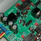
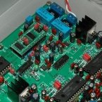
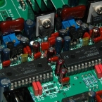
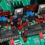
PMD100 to SM5842 Converter BD

Filed under: DAC — Spencer @ 9:21 pm

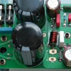
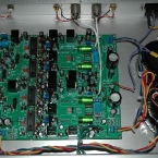
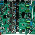
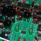
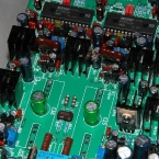
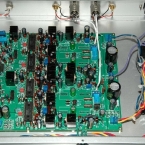
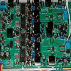
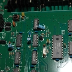
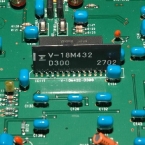
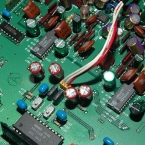
This is using PMD100 to replace SM5842 in D1Vx DAC.  The PMD100 can decode HDCD signal from CDs.

The input mode is right justified 16 bit and output is 20bit mode for PCM63.  All settings are hardwired and cannot be changed by jumpers!

Circuit

PMD100 pins asssignment

PMD100_BD Other Doc

Related Images:
January 2, 2008

Alesis AI-1 Sample converter

Filed under: Pro Audio — Spencer @ 4:39 pm

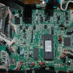
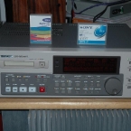
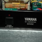
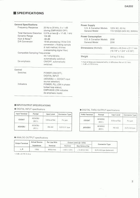
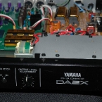
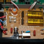
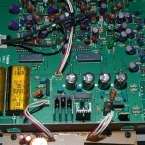
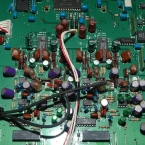
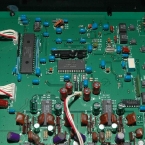
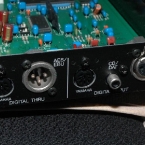
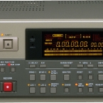
This is an old sample converter and digital selector for optical, SPDIF & AES formats.  The sample frequency can be selected for 44.1kHz or 48kHz.  Since this is old and you can get is as low as US$100 from ebay.

I use this to connect from my CD-PRO2 transport, SB3 or DAT as input and output to my D1V3, and other DAC or DAT.  This make my switching among equipment more easy.

Here are the photos:

Related Images:
October 11, 2007

DIR9001 to CS8412 Converter BD

Filed under: DAC — Spencer @ 12:33 am

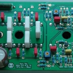
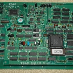
This converter board is to replace CS8412 in my DAC project D1.  This is designed to be used in the D1V2, D1V3 and D1V33 versions.  There are other DIYer who is interested to use this to replace the CS8412 in their DAC.  I have tested that it can be used to drive SM5842, SM5847, PMD100 and TDA1541 etc…  Take note that even through it is working fine but the output logic for DIR9001 is only 3.3V while all the old ICs are at 5V logic.  ACT logic should be used if 3.3V logic is needed to buffer up to 5V.

Another important note is the EMPH (pin 3) output in DIR9001 Converter BD is High when the data has pre-emphasis data added.  In a CS8412 or CS8414 chip, the pin 3 is LOW when the data has pre-emphasis data added.

The major improvement in DIR9001 is the lower jitter of 50ps (200ps for CS8412/14).  The improvement is very obvious in sonic performance of any DAC.

Sorry all sold out!

DIR9001 converter board Manual

DIR9001 converter bd BOM

9001 to 8412 V3 Circuit Diagram

Related Images:
August 8, 2007

F4 – Amplifier

Filed under: Pass Amplifiers — Spencer @ 9:47 pm

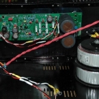
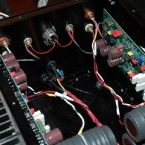
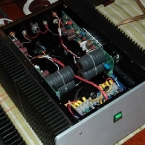
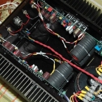
This is my F4 amplifier completed in August 2007:

  1. I designed the PCB and Casing myself and get China factory to custom make for me.  The casing size is 350mm (W) x 420mm (D) x 200mm (H) with front plate 10mm larger than the casing.
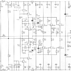
  2. R3 and R4 still 22 ohm, and Q1 and Q2 are using 2SK170BL and 2SJ74BL for matched Idss to within 9.8 to 10mA.
  3. C1 to C4 use 330uF 35V Panasonic FC, gate resistors R10 to R15 are 100 ohm, Source resistors R16 to R21 are 0.51R 3W.
  4. IRFP240 and IRFP9240 are matched Vgs within 5mV which give variation of bias current within 5% (measured voltage at 0.51R 5% resistor) among all the mosfets.
  5. Use two 18V x 2 250VA transformers and 4 birdge rectifiers to parallel the secondary voltages to about +/-21.8Vdc with 1.45A bias for each channel.
  6. Filtering capacitors are Nichicon 68,000uF 63V x 2 + 0.47R//4 pcs + Mallory 33,000uF 35V x 4.
  7. Heat sink size is 420mm x 200mm x 50mm for each channel (side).  Temperature rise is about 17 deg C (i.e. 47 degC for room temp of 30 degC).
  8. The DC offset is stable to be within 10mV after warm up for 1 hour.
  9. Measured distortion is 0.02% at 1W output for both Channels.  Noise is mainly at low frequency band from 25Hz to 1kHz.
  10. The F4 amplifier has been playing for 4-5 hours a day in the pass week and the sound is already stable.  The sonic is skid to soft type bass (due to limited power) and clean and clear mid and high frequency.
  11. Overall the sound is very good and satisfying.

Some photos below:

FFT measurement at 1W and 20W:

F4 FFT2 1W 8ohm

F4 FFT 20W 8ohm

Related Images:
June 8, 2007

Jfet IV Board

Filed under: DAC — Spencer @ 9:33 pm

* * Sold OUT in 2009 and no more selling * *

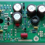
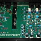
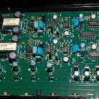
This Jfet IV board was released in 2007.  The purpose of it is to modify a DAC or CD player IV converter.  It can be used for most current output DAC chips like PCM63, TDA1541, AD1862, PCM1702, PCM1704 etc…  NOS DAC is not recommend to use this Jfet IV due to excessive high frequency noises.

During the time of release, 2SK170 is used as the active device for IV.  It is now recommended to use 2SK369BL as the active device due to its higher gain around 40mS for better result.

Jfet IV Circuit

Jfet IV BOM

Related Images:
« Newer PostsOlder Posts »

Powered by WordPress