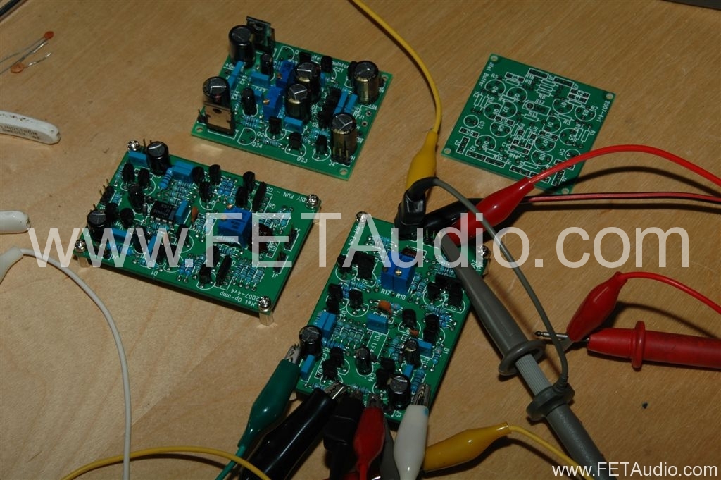
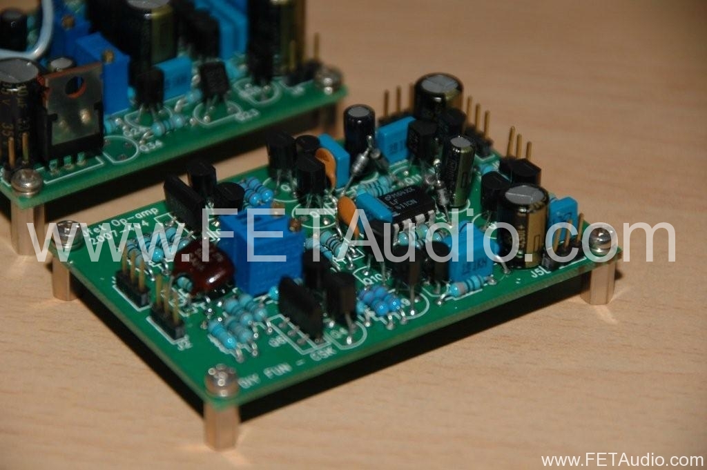
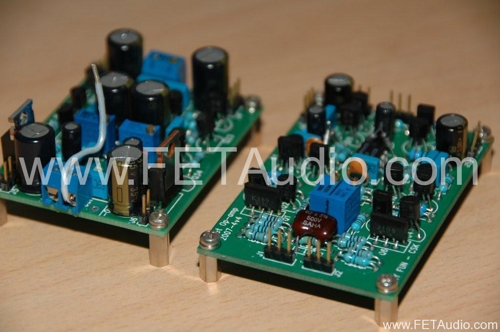
This is another Borbely Erno design op-amp using all jfets. This is the most complicated one with high gain and thus a servo is required to maintain the output at near 0Vdc. I have tried this op-amp but I have not make it up to the best sound. As of 2009, I think the all jfet buffer line amp sound the best.
May 16, 2007
April 30, 2007
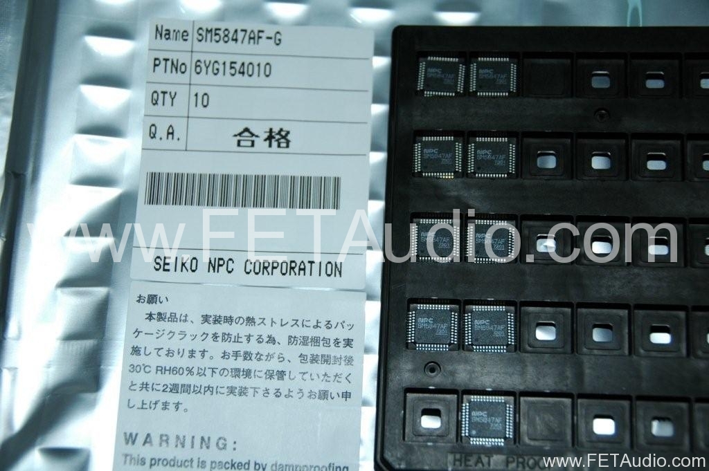
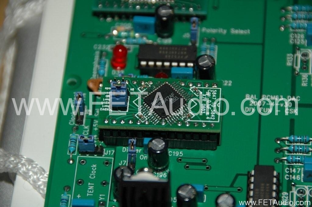
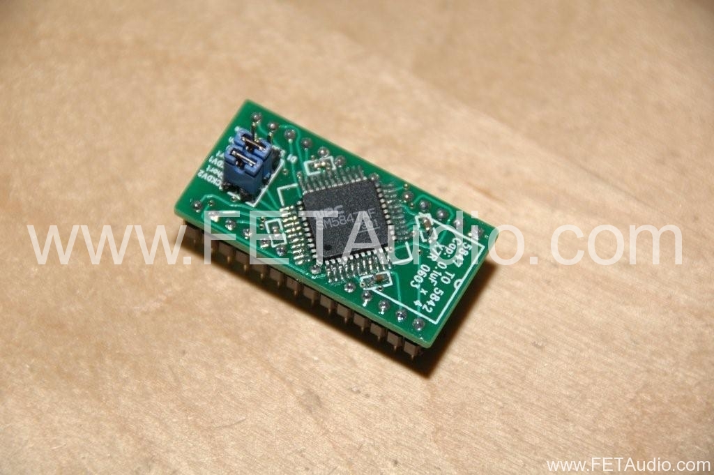
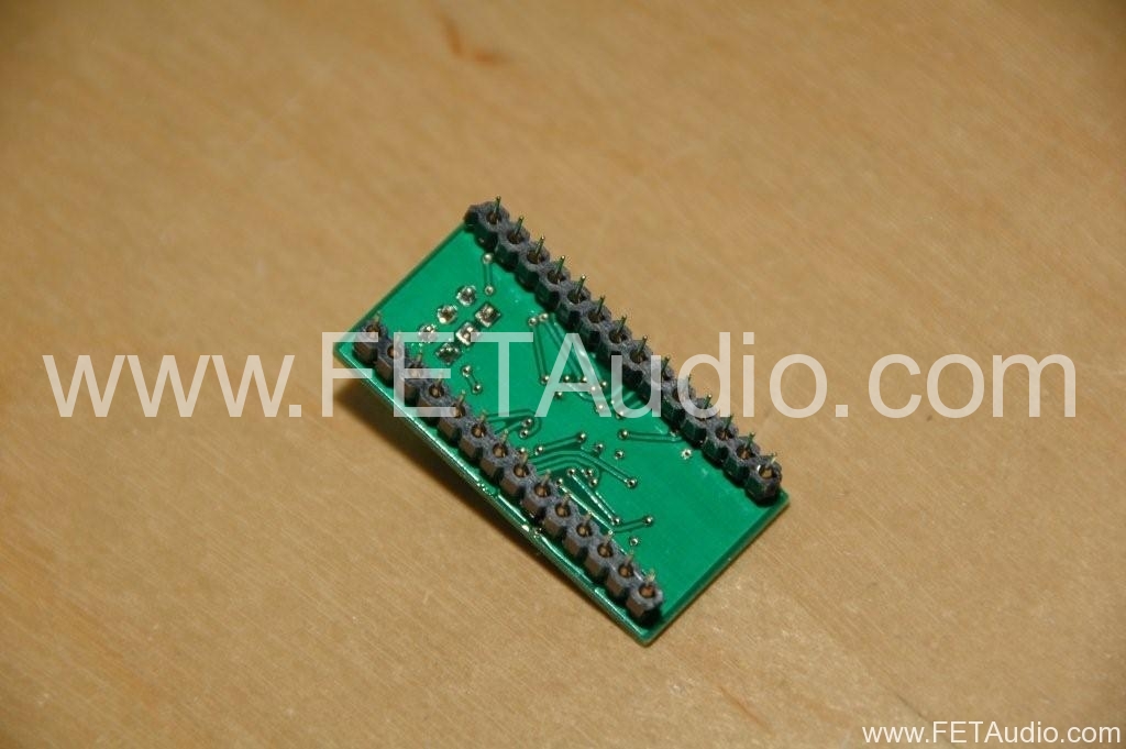
SM5847 to SM5842 Converter BD
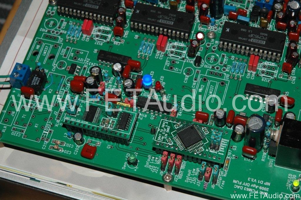
Update on Dec 31, 2009: Add photo on D1V33 jumpers setting with 24 bit input upgrade.
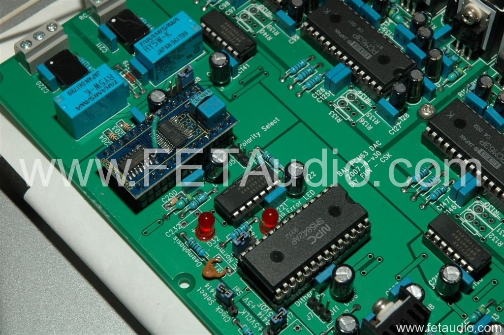
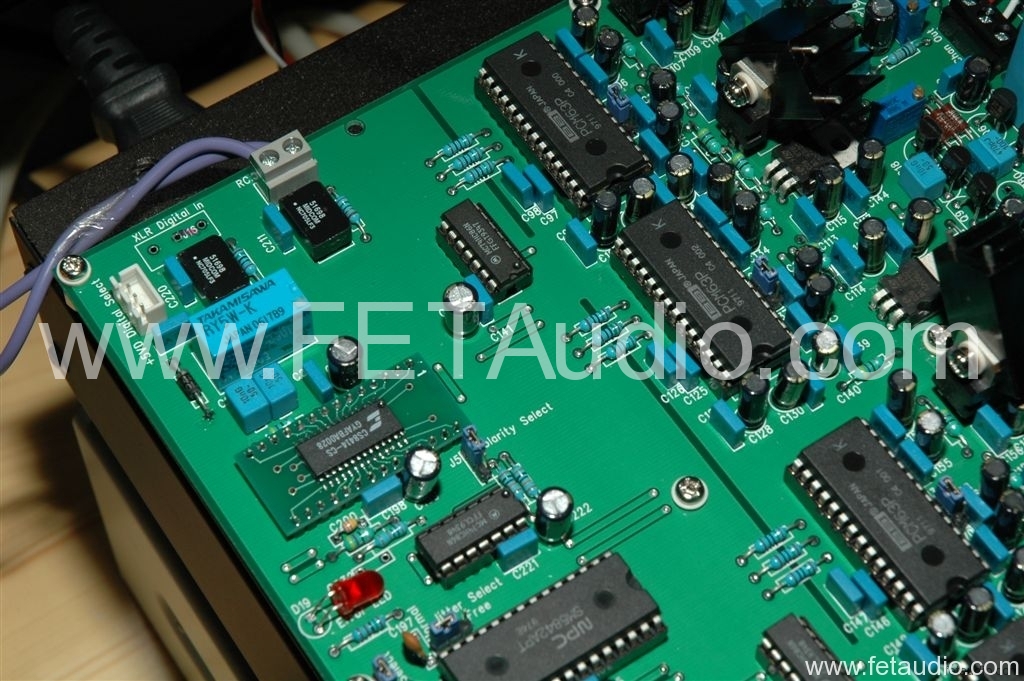
The converter board use SM5847 to replace obsoleted SM5842 digital filter. It can be used in any version of D1Vx pcb. Photo is on a D1V2 pcb.
Related Images:
April 22, 2007
D1V2 DAC
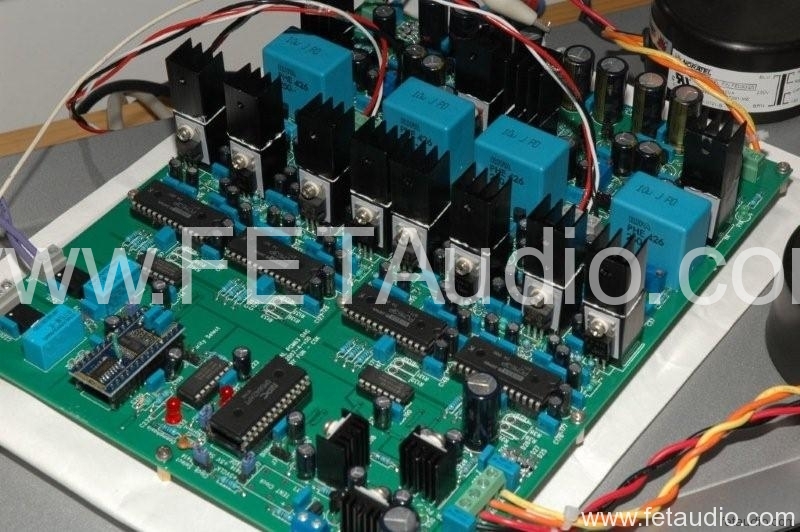
This is D1V2: Changes from D1V1 is listed below.
- Add a super clock (11.2896MHz) output socket pad (J20). This is reserve for the clock to feedback back to CD transport.
- Allow more space and add holes for all TO-220 heat sink (total 15 T0-220 parts).
- Add one more relay to select digital input (K2). Use jumper to select either XLR or RCA input (J8).
- Short circuit the PCM63 Iout to BPO and thus no more jumper is required (J1-4 are eliminated).
- Enlarge all hole/pad sizes.
- Add a ground connection for the ground plan on top near main filter capacitors (J19).
- Jumper to select the “clock regulator” or “5842 regulator” for the 8414 IC (J17). Thus the regulator for 8414 will be isolated from 5842 when the on board clock is not used.
- Use LM317T and LM337T regulators (better noise performance) for all DAC chips.
- Add de-emphasis LED indicator (D32).
- Split the ground plan in sections: 8414, 5842, Input relay and logic IC, DAC left and DAC right.
- Relocate the rectification section (diodes and caps) of the 30V supply so that the last few filter caps will be closed to a centre ground point J19.
- Add “+” mark for all E-capacitors for easy polarity identification.
- Add resistor and VR for all PCM63 to trim the MSB (this adjustment is optional and reserve for DIYer to play around the trimming of MSB).
- Add Trimmer pot (R8, 9, 17 & 18) to adjust Jfet IV output level to match “+” and “-“ cycle. This is also optional and need an accurate voltmeter and test CD to do the adjustment. Do not solder the parts if not use.
Documentation:
Related Images:
March 14, 2007
Step Attenuator
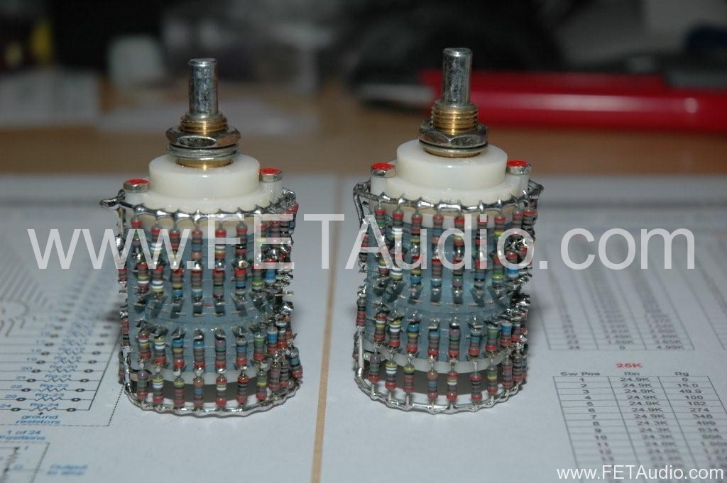
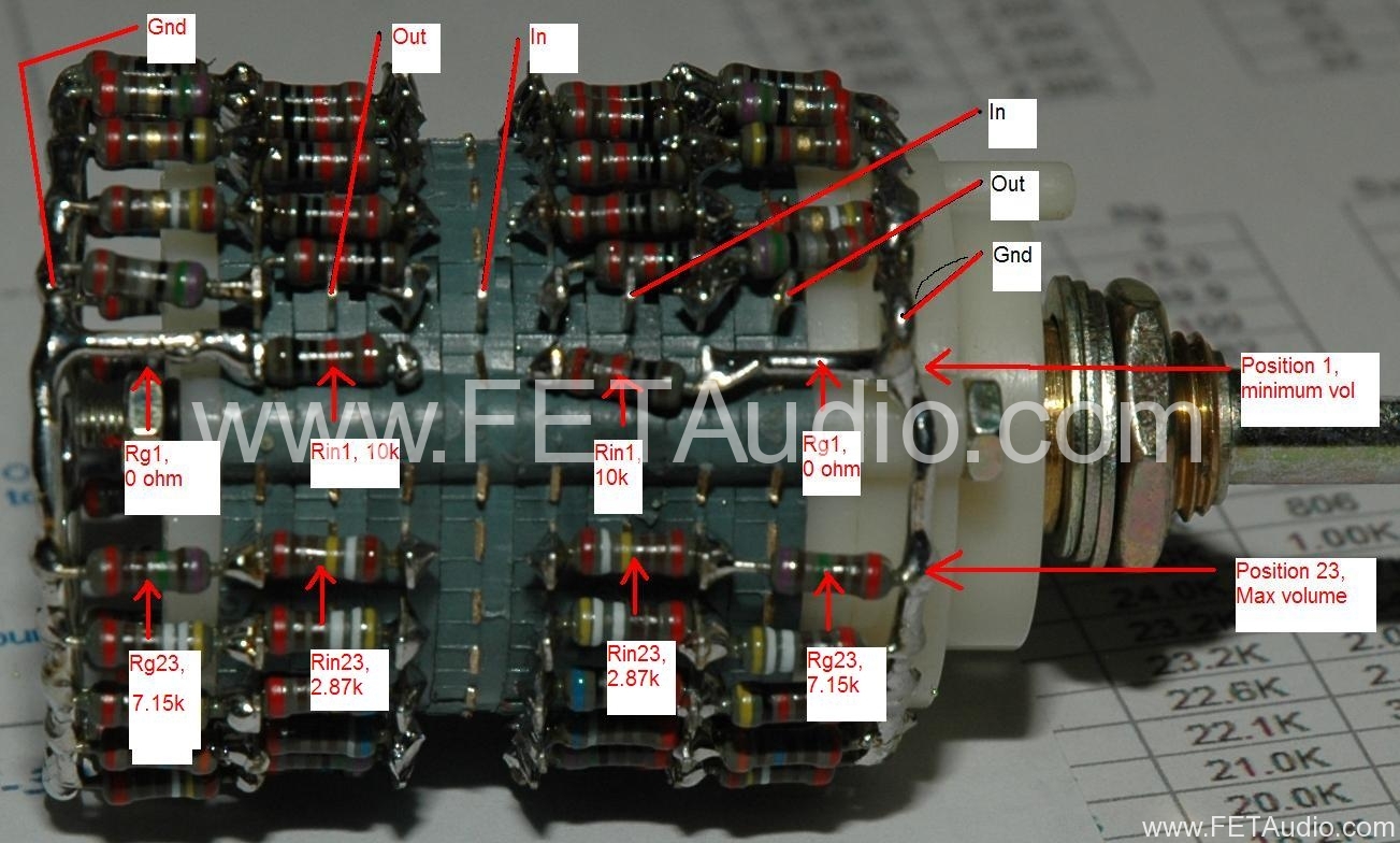
This is a ladder type step attenuator used in my pre-amp. The switch is a 23 throw 4-pole and thus it is good for one balance channel.
Related Images:
March 9, 2007
D1V1 DAC
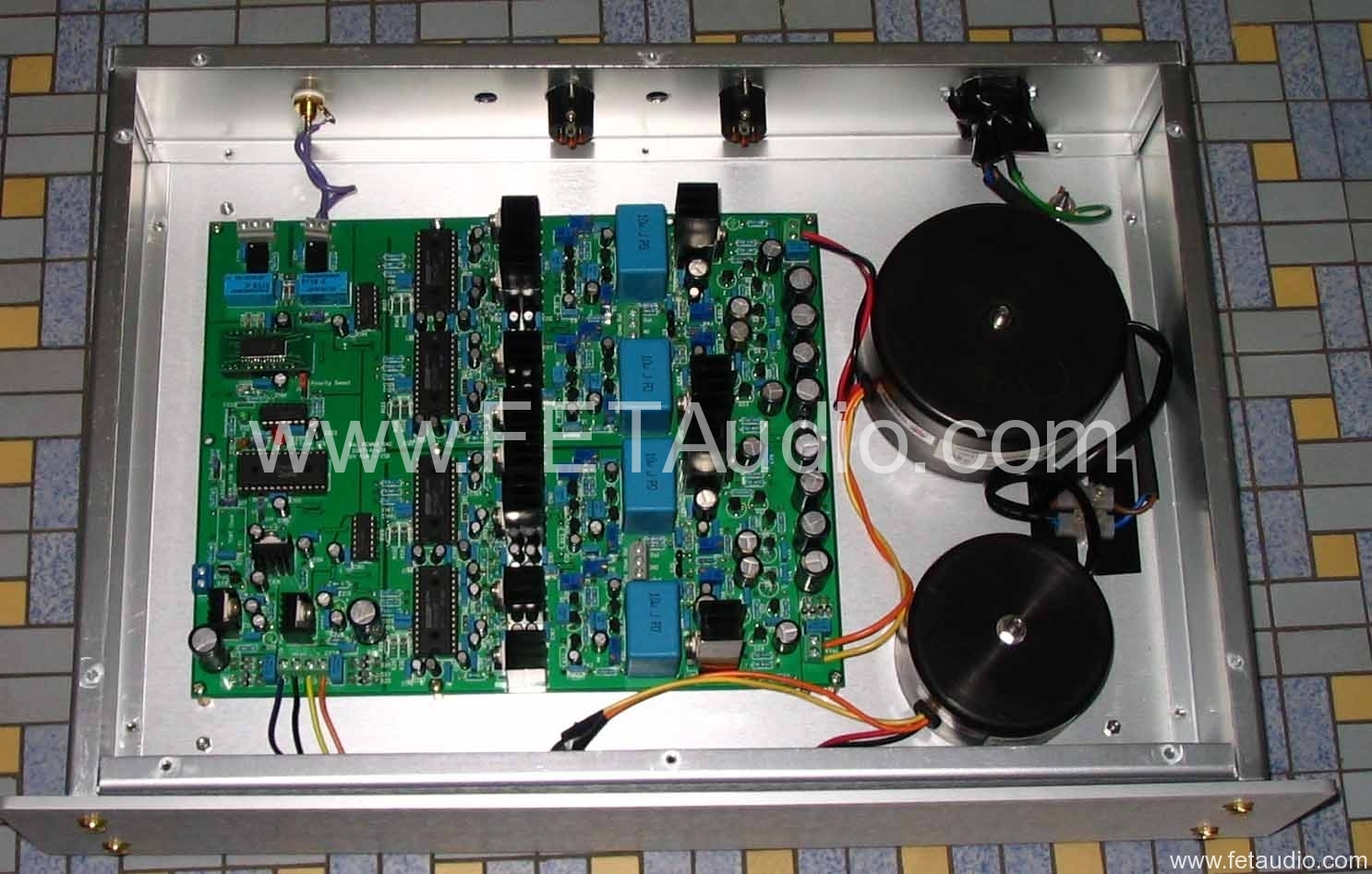
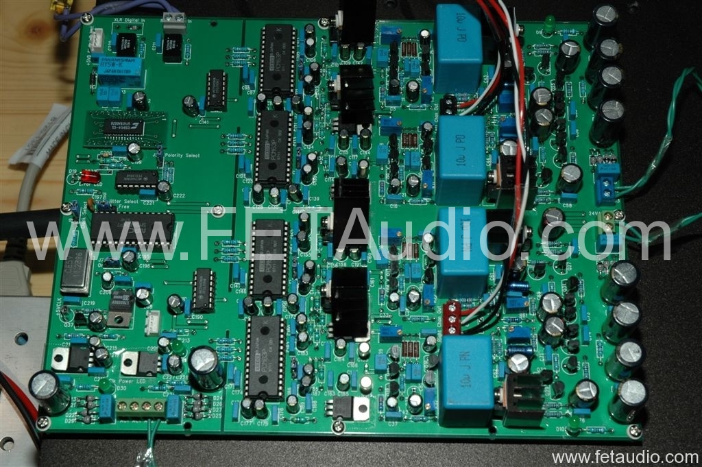
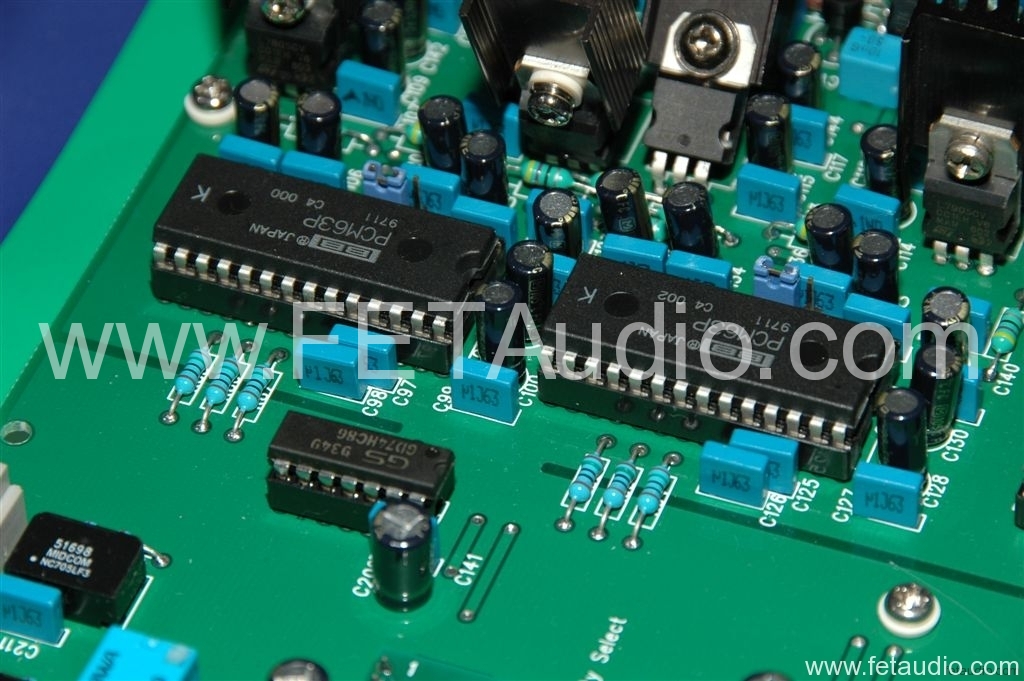
D1V1 was the first revision of clone NP D1 DAC. It has CS8412 or CS8414 (on daughter board) digital receiver, no 2nd PLL, SM5842 digital filter, 4 x PCM63 in balance mode and Jfet IV (not mosfet IV). All regulators were using normal 78/79 series 3 pin regulator ICs in digital and DAC section. Two discrete low noise regulators were used in the Jfet IV section. This DAC was made as a trial version on jfet IV back in 2007. The benchmark of this DAC at the time was a Lite DA-50 DAC with PCM63P-K and 6922 tube IV. This D1V1 won the Lite DAC in smoothness of sound, noise level and image.
Silkscreen Top view: