FET Audio | Hi-End Audio & Electronics DIY Electronics & Repair

January 30, 2022

D1V33 + Zen I/V re-visit

Filed under: DAC — Spencer @ 10:47 pm

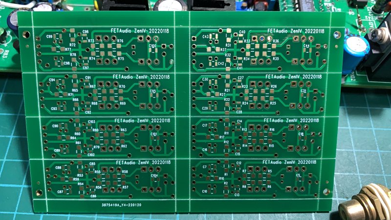
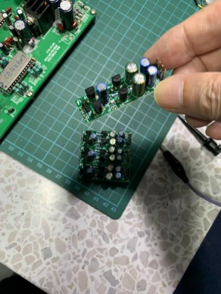
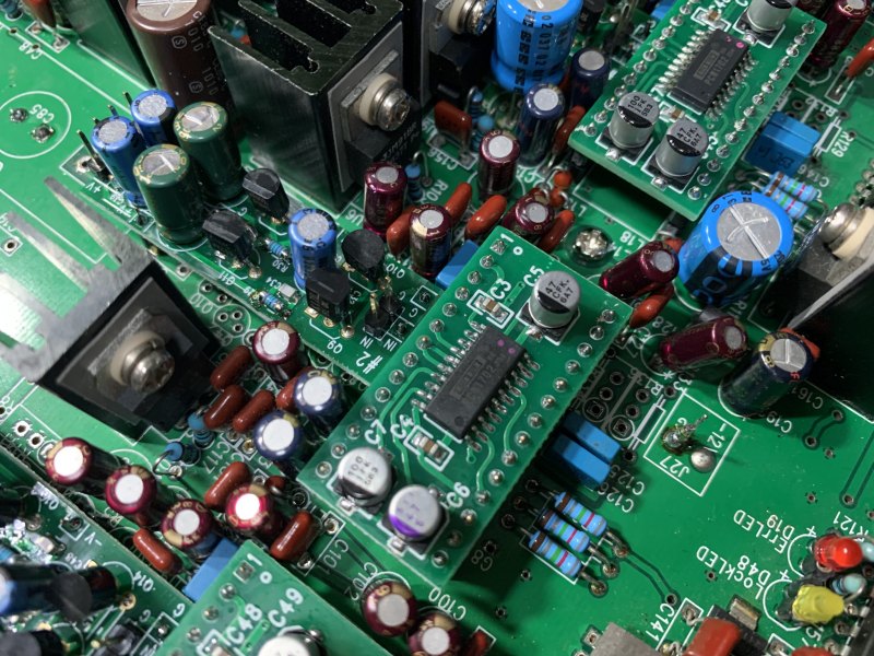
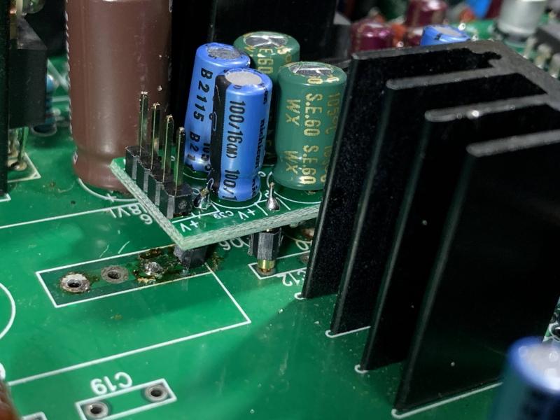
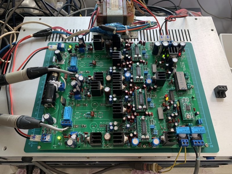
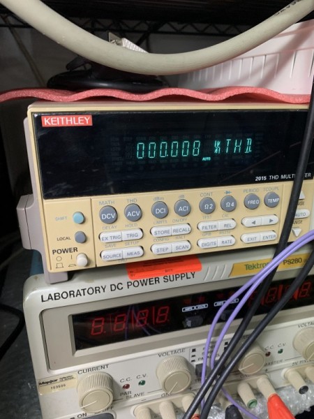
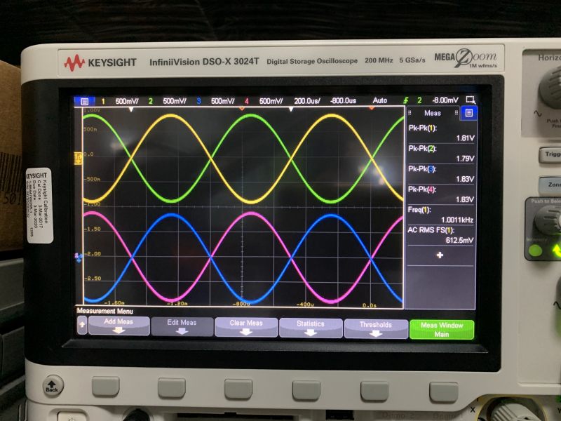
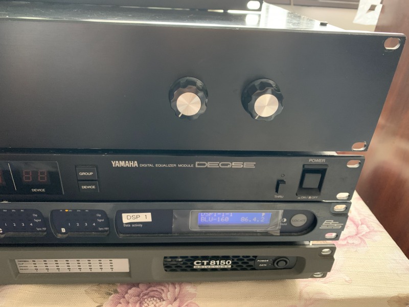
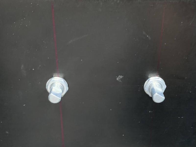
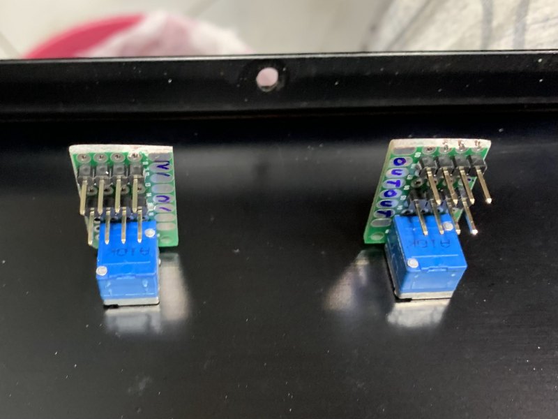
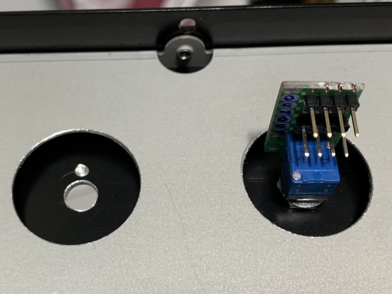
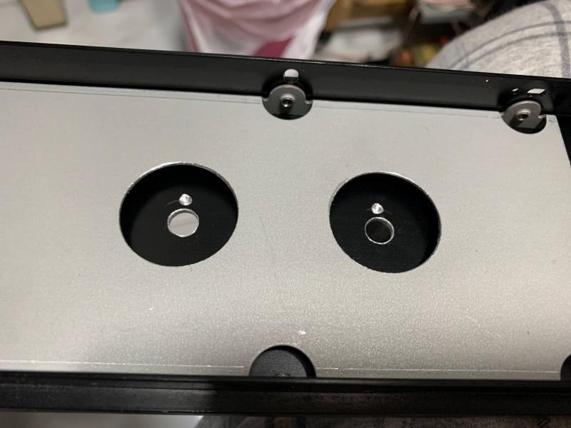
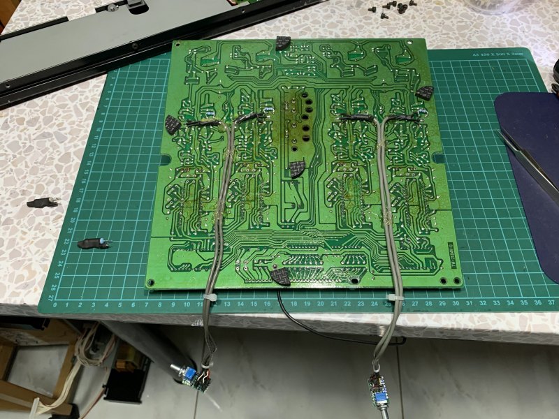
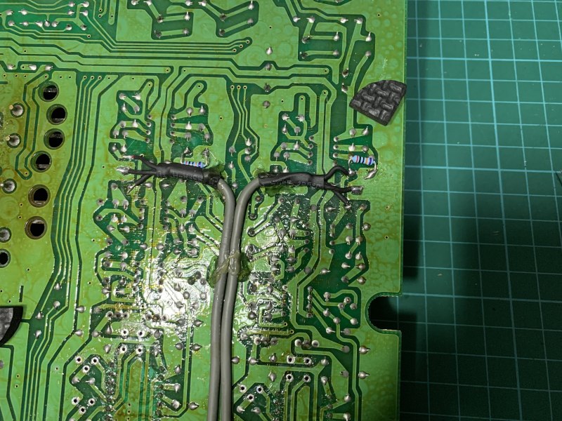
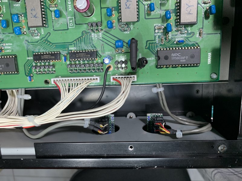
The Zen I/V was posted by Mr. Nelson Pass back in 2010.  I have not enough time to try that due to my work location change and far away from my equipment.  I am back home since 2021 and now it is time to try out the Zen I/V.  Below is the photos of the Zen IV that I put on the D1V33 board and so far the result is very positive. The distortion for SE measurement can be down to 0.002% to 0.004%, in fact that is the distortion spec of the DAC chip.  Here is the information sharing for anyone interested to comment.

  1. Rail voltage is only +/-20V as it is the limit of the current D1V33 board default supply. 
  2. Use Drain resistor of 1.5k ohm due to limit of the rail voltage and thus give a Vd about 7V for jfet Idss of about 8mA.  This is compromise due to Rail voltage max at 20V.
  3. Use daughter boards to put on top of original jfet IV locations.  Since the pins for supply, input and output are not the same, thus I have to design 4 similar boards with different locations of the pins.  The boards are names #1 ~ #4 for identification.  Daughter Board is connected to main board via pins, some holes are not really on top and thus the pin has to be soldered a bit tilted (best locations of pins).
  4. Emitter follower is added to the Zen I/V with a pair of transistors to buffer the output to have lower output impedance.  The distortion so far do not see any degrade in readings.  In fact jfets pairs can be used but it will increase the cost!
  5. SMD resistors 1206 or MELF 1/4 W and capacitors 0805 are used on top and bottom of boards to make the board as small as possible.
  6. Tough job is to remove the original Jfet IV parts on the main board and it is helped by a de-solder station make by YiHua 948 (about US$60).  SMD part is soldered with hot air gun also YiHua 8786D 2-in-1 station (about US%65).  Really handy tools and cheap!
  7. I still left some pcbs and thus those interested, I can send to them with cost of SGD$20 for each set (include paypal and shipping cost).  Sorry I do not have any more K170/J74 match pairs for sell!
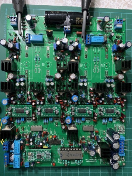
My version of Zen I/V circuit: D1_V2_2_ZenIV_ckt

3D view of the Zen I/V board: D1_V2_2_ZenIV_3D
Related Images:

December 9, 2021

hp 339A distortion meter

Filed under: Test Equipment — Spencer @ 2:09 pm

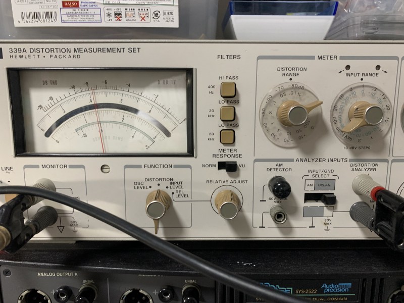
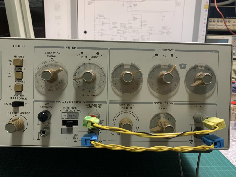
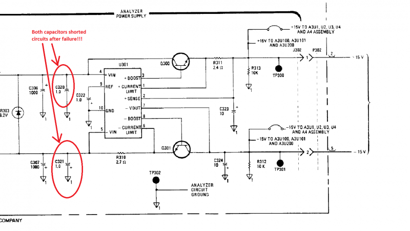
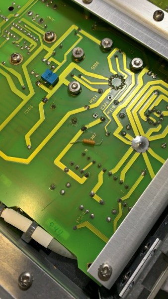
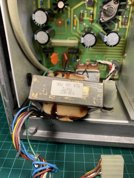
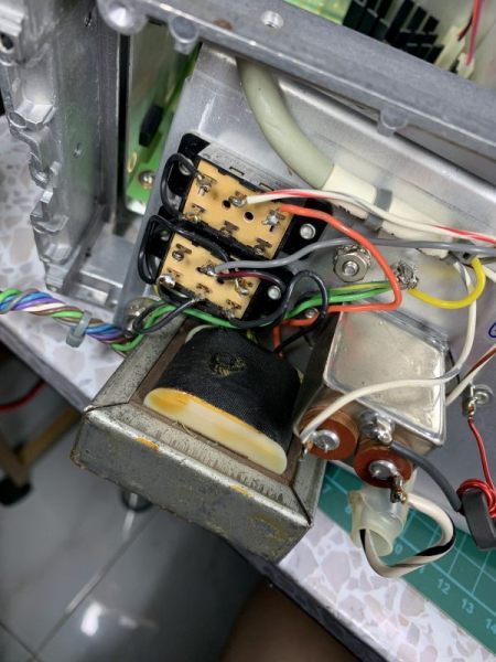
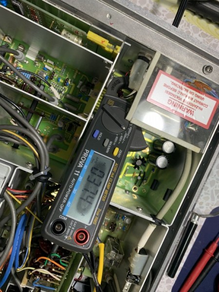
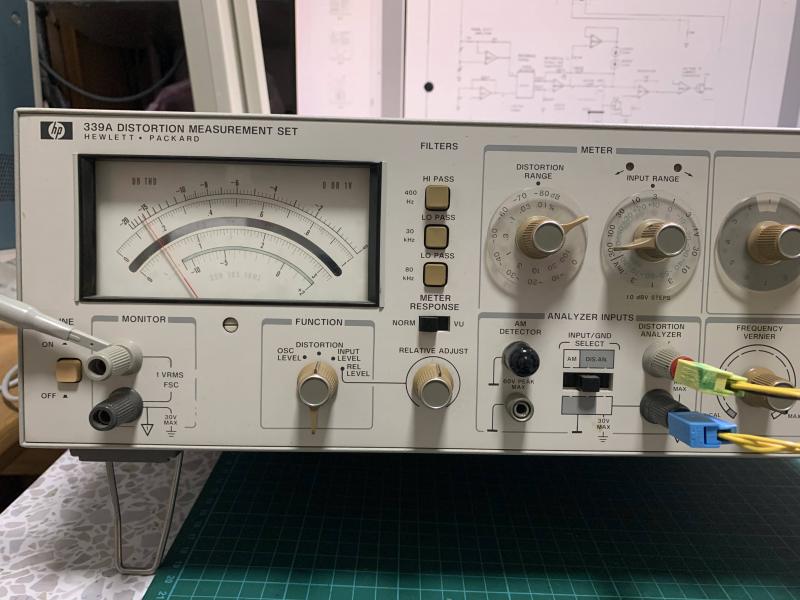
I acquired this machine for more than 10 years and was defective due to transformer spoilt (super hot) and burnt fuse about 3 years ago.  I did not have time to repair it since then.  Recently I saw a transformer on sales on ebay and thus I purchased it and make replacement.  Reason for the failure is the capacitors C320 and C321 short circuit in the power supply section.  I put back two film capacitor 0.68u 63V type.  Here are the photos of the repair for reference.

Related Images:

November 18, 2021

Tektronix 577 curve tracer repair – Collector Supply Disable Light ON at 6.5V and 25V positions

Filed under: Test Equipment — Spencer @ 7:52 pm

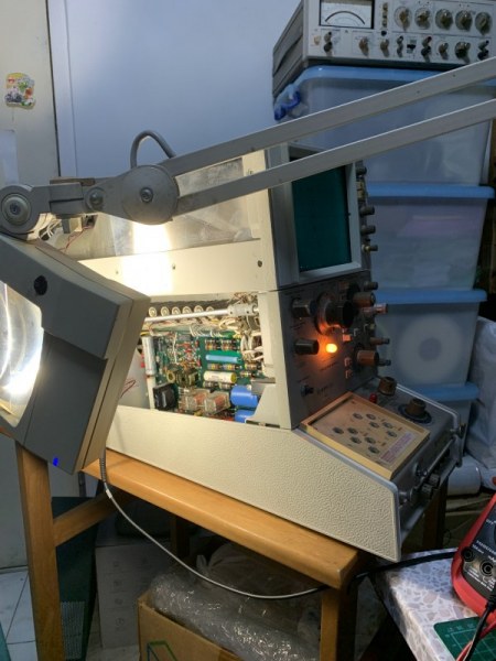
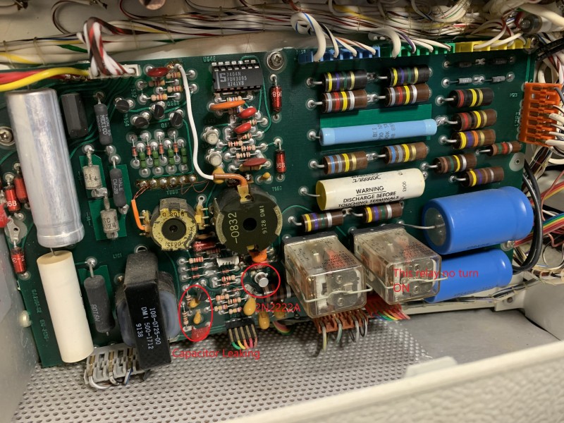
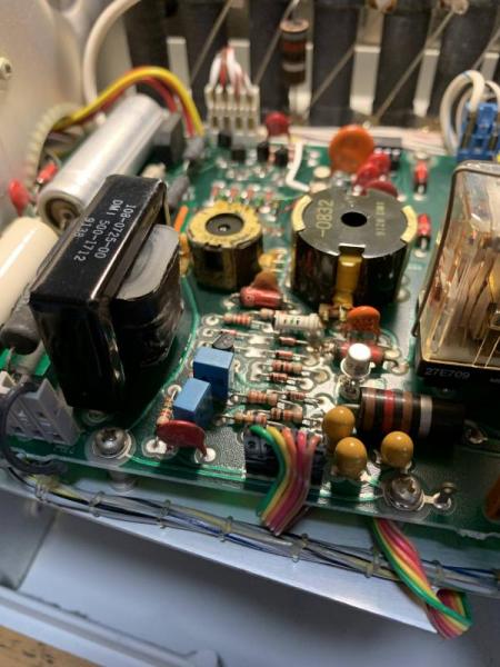
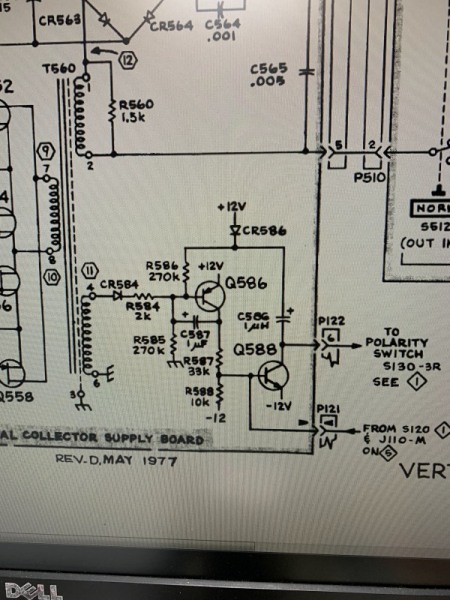
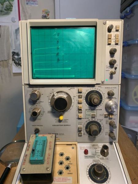
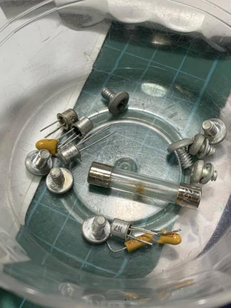
The Tek 577 curve tracer is more than 25 years and components start to fail from time to time.  The symptom is front YELLOW light ON (Collector Supply Disable Light)  after power on and cannot output any voltage.  After tracing, the circuit, the reasons is due to K115 not turn on, due to K125 not turn on, due to Q588 open.  Replace new 2N222A to Q588 but always burnt (try 3 pcs) after power up!  Later check base voltage is at 6.xV dc which is too high relative to Emitter at -12V.  Thus transistor will be burnt after power up.  Check Q586 is fine and then after removing Q586, the base at Q588 is still very high voltage.  Thus suspect C587 defective (leaking).  So change C587 by using 0.68 + 0.47 = 1.15uF (original is 1uF) from Tant to film capacitor.  Also change C586 as it may also be defect soon.  After plug in Q586 and Q588, the set works again!  Here are the pictures of repair.

Lesson Learnt: Tantalum capacitors when failed, it always leaking or even short circuit!

Related Images:

October 22, 2021

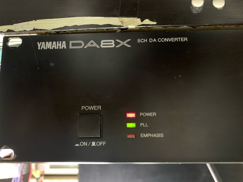
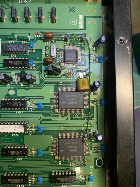
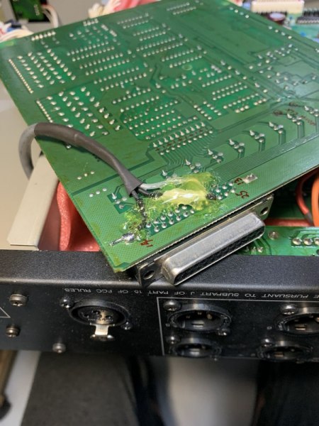
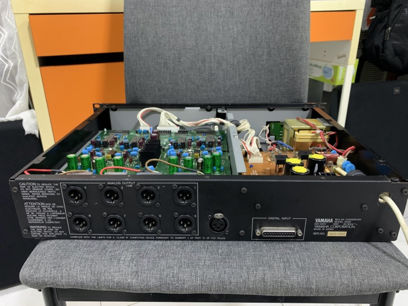
Yamaha DA8X convert from Y2 to AES digital input

Filed under: DAC,Pro Audio — Spencer @ 10:15 pm

Total I brought two of these DA8X but I never have chance to hear the music from it.  Here is what I do to make it works:

Details modification procedure (New V4): Yamaha DA8X Modification from Y2 input to AES input v4

Data sheet: YM3436

Draft: DA8X draft notes

DA8X service manual: https://www.synthxl.com/yamaha-da-8x/

Bourns Pot: Bourns 10kA 1874875

Related Images:

July 2, 2021

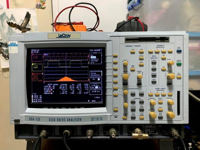
LeCroy DDA-120 Repair PS, LCD upgrade and add software OPTIONS
Filed under: Test Equipment — Spencer @ 12:43 am

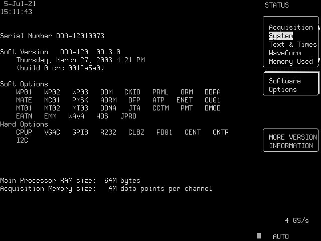
You can see I have added many options of this scope (>95% full). The information can be found in EEVblog and look in below link reply #85. The difficult part is for me to install Python2.7.18, Visual Basic for Python2.7 and PyCrypto in my Windows 10 PC to run the Python scripts.

https://www.eevblog.com/forum/testgear/lecroy-options-recovery/75/

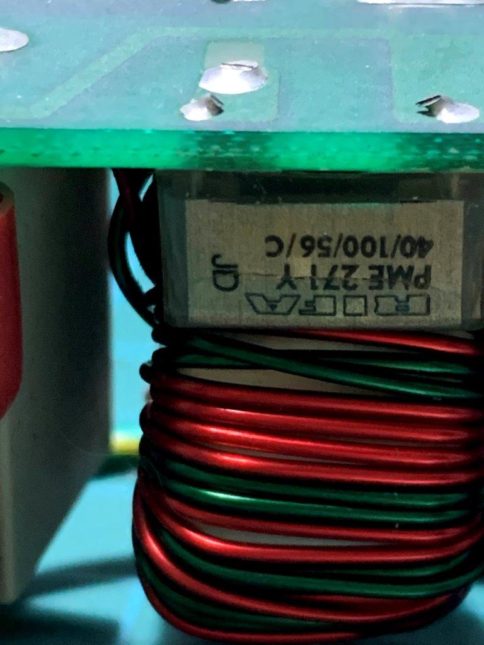
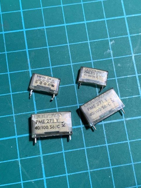
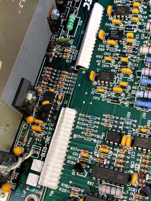
  1. Power supply is leaking due to RIFA PME271 capacitors (4 pcs in supply filter circuit) leaking (body crack). Change to other type High voltage safety capacitors to prevent leaking. Also -15V supply is not stable and I replace U3B LM358 op-amp by normal JRC5532 to resolve the issue. +15V supply retune and get back +15V from 8.xV. The supply design is not really good as it use some TO-220 power transistor and load resistor to drain the power supply to get the rated voltages but if the supply is not connected to nominal load, then it may be over-voltage a bit and loading transistor will be super hot!
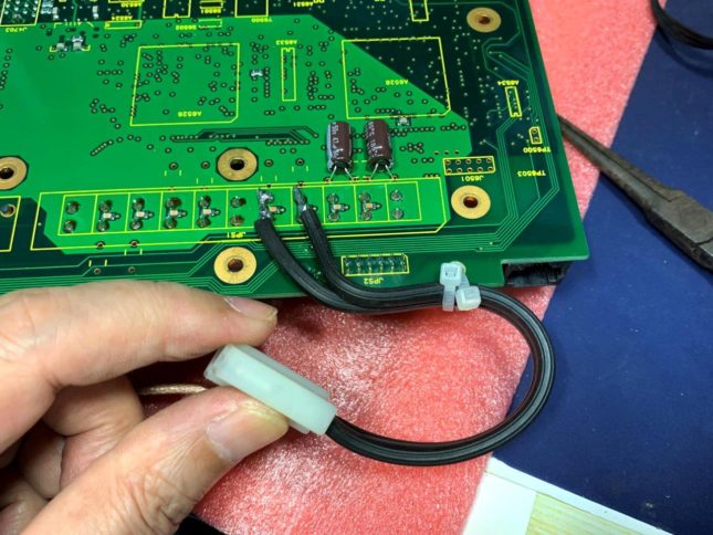
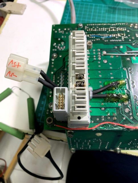
  2. The connector from power supply -5V is oxidized and darken and thus bypass wires are added with plug & socket for both +5V and -5V to ensure good conduction.
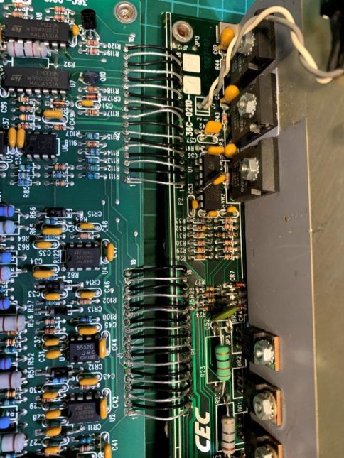
  3. The regulator also has two jumper wire cables for connection and I found that these single strand wires are very easy to break (brittle) and thus I changed them to Telfon stranded wires to increase the flexibility & reliability. Reasons was that I experienced the +/- 6V from regulator loss its regulations and output +/-12V to the main board due to jumper connection open or intermittent!!! This will make the scope cannot acquire signals and relay keep on clicking with channel 2 missing trace, cannot reset scope and offset adjust unstable. Very danger to further damage the main board if not power off immediately.
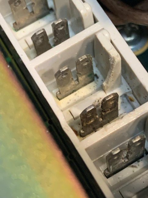
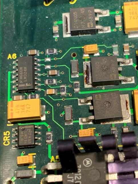
  4. After the supply issue on +/-6V become +/-12V, I found there are two Mosfets (D14N05) on the main board become brownish and solder joint looks overheated. The symptom is that the scope failed like item 3 after warm up a while. Thus I re-solder them again on the PCB to resolve the issue. Photo shows that the solder is a bit melt with darken flux residue mark and looks like cold solder joint!
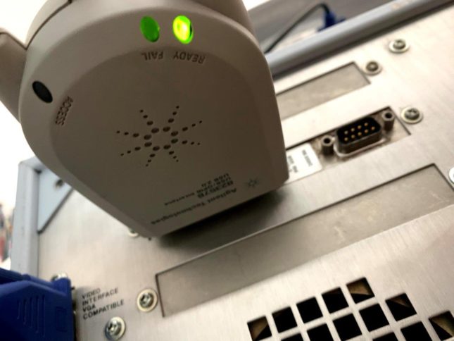
  5. I use Agilent 82357B GPIB adaptor and after install the driver, MUST enable the IEE488 function or else it cannot work due to default to Keysight equipment only!
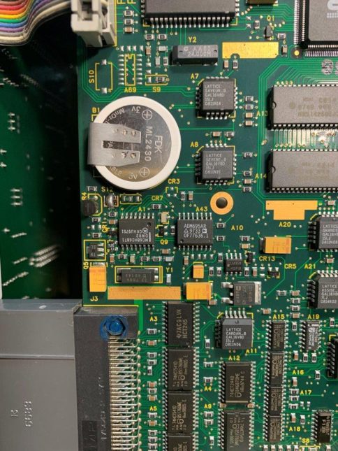
  6. Battery is replaced with same type rechargeable (about US$8).
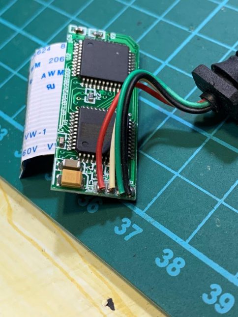
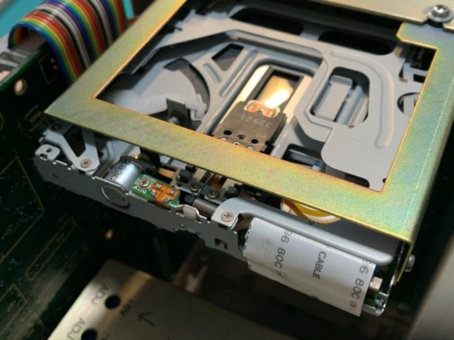
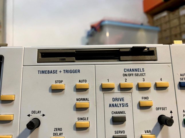
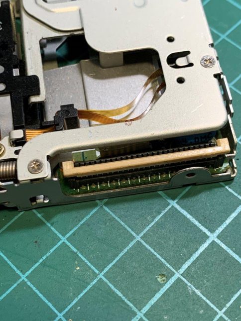
  7. Floppy drive is also replaced. I own an old no brand USB floppy drive about 10 yrs ago (IBM brand USB floppy is pure USB design main board; Non IDE version) and open up see that there is a USB to IDE converter PCBA. In fact the drive is an IDE floppy + USB convertor board and the connector 36 pins just fit into the original mounting kit, excellent! I need to cut and filing away some plastic on the front panel and also glue the original plastic front cover on to the front panel to fit, looks quite nice!
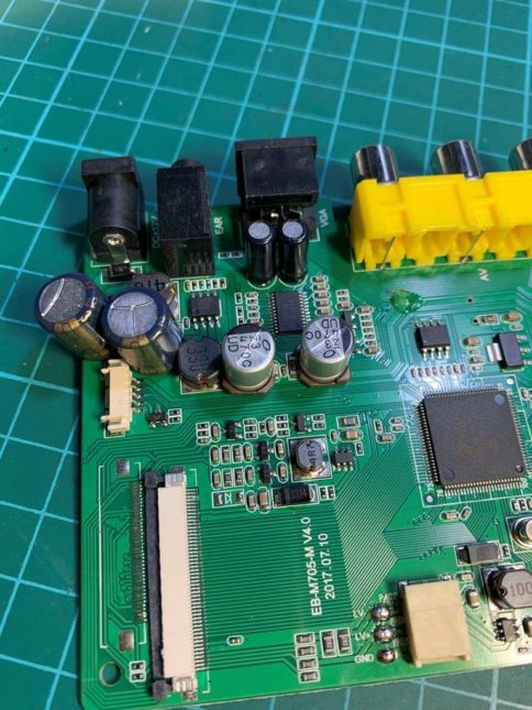
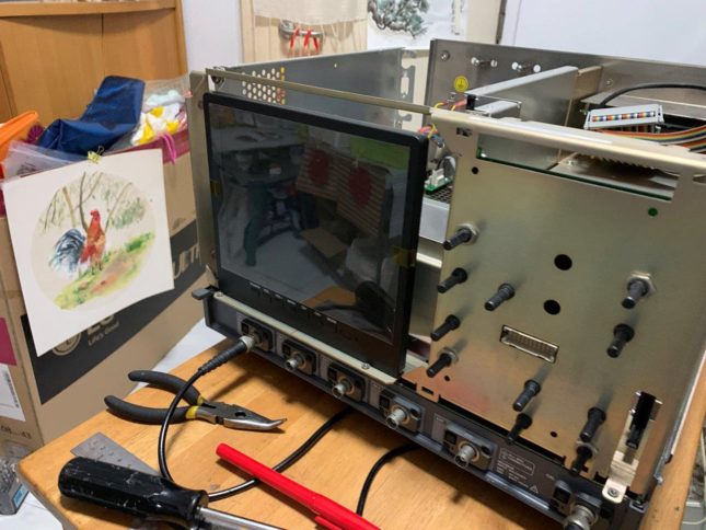
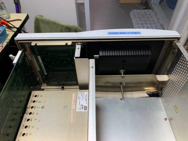
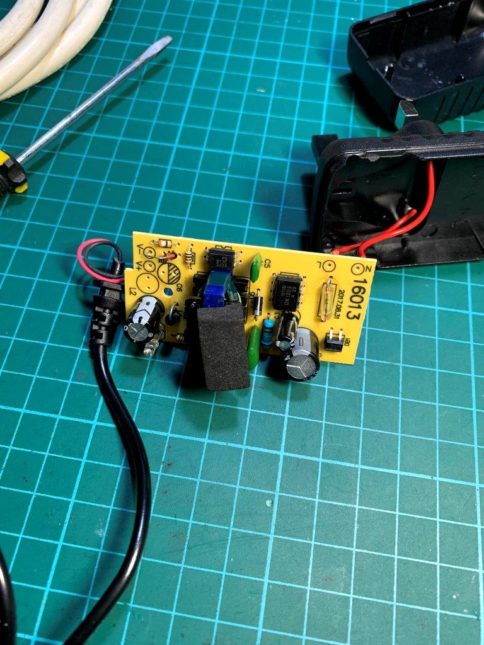
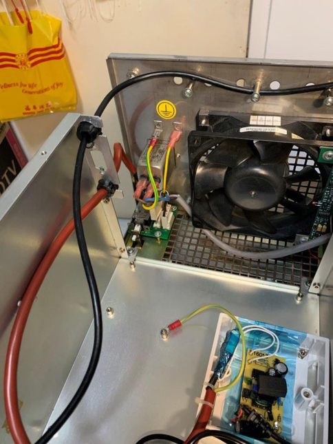
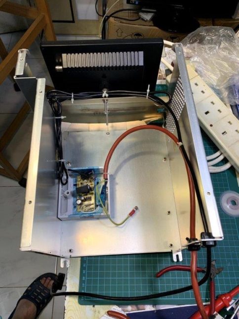
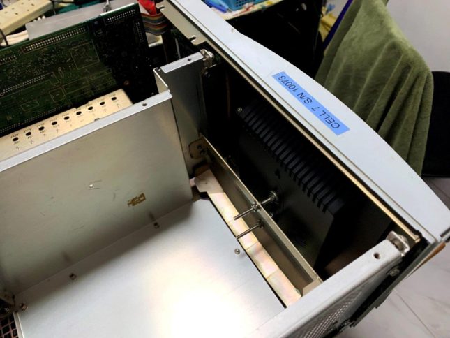
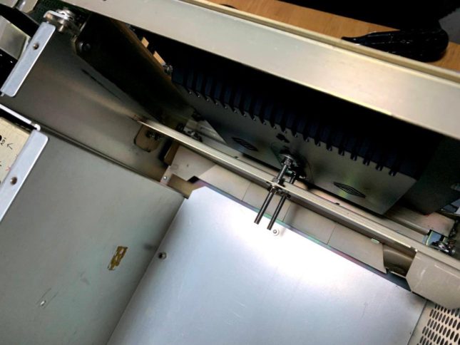
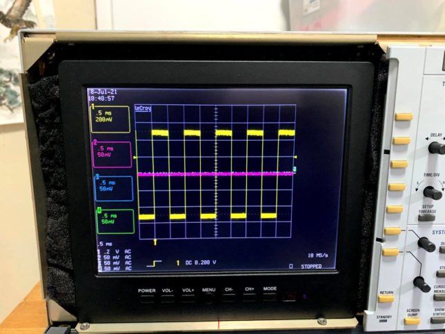
  8. I have changed the display from picture tube to LCD monitor! The LCD monitor only costed me US$30 and all E-caps are upgraded to Panasonic FC in both LCD main board and the AC adaptor. Note that the monitor need to be 8 ~ 9 inches screen size with 4:3 aspect ratio and VGA input must be compatible with resolution 640×480. Picture show how the LCD is installed using the bottom curved metal frame for mounting the LCD monitor back by drilling two holes on each side to secure in position. Two long screws are used to support the back side of the LCD monitor slot and mounted at the center of the curve metal frame. LCD monitor power Adaptor is open up, changed all E-cap to better grade and put the PCBA in an electrical plastic box for better cooling. Original power cable is used and monitor VGA cable from monitor is routed through original back hole positions for connection to Power Switch point and internal VGA out.
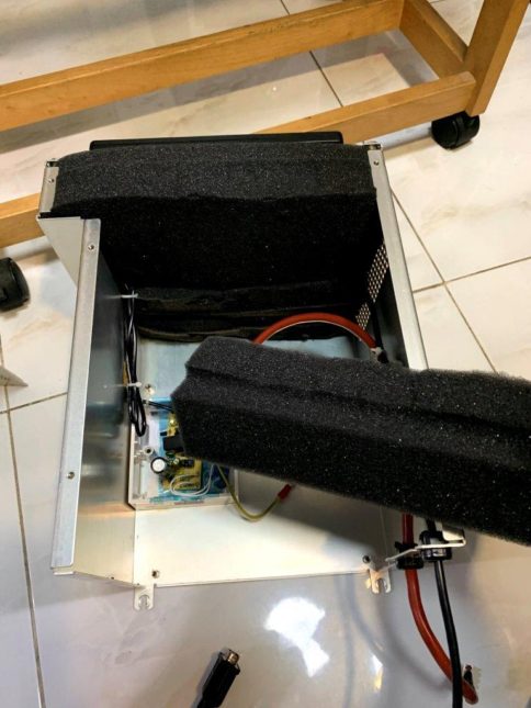
  9. The display metal box is totally re-used and put back into the scope same position. This is necessary as the mechanical strength is maintained for the chassis especially the front panel mountings! I added a PP sheet at the back of the TV box to block all the holes there for TV section air circulation. Thus the internal airflow for big fan is now mainly from the bottom main board (believe a bit better than before). Overall the fan noise is still there and I added some acoustic foam behind the LCD monitor as shown and it can reduce a bit the fan noise!
  10. The thermal printer is still working but I feel there is no need to keep it and I totally remove it and use a plastic sheet to cover up the top rectangular hole to ensure air flow is same as before. So in total I can reduce the scope weight by almost 5kg and consume less 100W power!
  11. Serial number is re-written by Lecroy Explorer (Use “**SY_NO xxxxx”, one space after letter O) and firmware 9.3.0 is updated to the scope. Here I thank you very much the “LeCroy Owners’ Group” for providing all the service manuals and necessary information at below link. Without the group, my repair may not be successful! https://groups.io/g/LeCroyOwnersGroup

Related Images:

« Newer PostsOlder Posts »

Powered by WordPress